Faculty
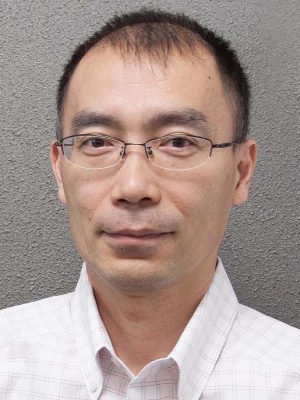
Hiroki Hibino
Major research activity
 Graphene and related two-dimensional materials, surface physics, crystal growth, surface microscopy
We are targeting to create new physical properties and functionalities based on graphene and related two-dimensional (2D) materials towards innovative devices contributing to sustainable development of our society. Graphene, a 2D sheet of carbon atoms, was experimentally discovered in 2004. Since then, owing to its fascinating properties, graphene is attracting intense attention both fundamentally and technologically. Besides, there are many other 2D materials with various properties, such as insulating hexagonal boron nitride and semiconducting transition metal dichalcogenides. We expect that 2D materials and their heterostructures will be utilized in a wide range of future applications.
Our research topics include growth mechanisms of 2D materials and effects of defects on the physical properties of 2D materials. Nanoscale characterization techniques are our strength. We tackle the understanding of the growth mechanisms through detailed structural analysis using various microscopes. The understanding will lead to high-quality 2D materials and heterostructures. But currently, real 2D materials have various types of defects such as grain boundaries, edges, and wrinkles. Defects can largely change the properties of 2D materials, and are also a potential source of new functions. Therefore, it is important to clarify how defects affect the properties of 2D materials. For this purpose, a technique of simultaneously resolving structure and electronic/optical properties at nanometer scale will play a key role. In the future, based on the high-quality materials and knowledge about the physical properties, we also aim at fabricating energy efficient electronic/photonic devices with 2D materials and evaluating their performance.
Major relevant publications
- S. Wang, S. Suzuki, and H. Hibino, “Raman spectroscopic investigation of polycrystalline structures of CVD-grown graphene by isotope labeling,” Nanoscale 6, 13838 (2014).
- C. M. Orofeo, S. Suzuki, Y. Sekine, and H. Hibino, “Scalable synthesis of layer-controlled WS2and MoS2sheets by sulfurization of thin metal films,” Appl. Phys. Lett 105, 083112 (2014).
- M. Takamura, H. Okamoto, K. Furukawa, H. Yamaguchi, and H. Hibino, “Energy dissipation in edged and edgeless graphene mechanical resonators,” J. Appl. Phys. 116, 064304 (2014).
- S. Wang, S. Suzuki, K. Furukawa, C. M. Orofeo, M. Takamura, and H. Hibino, “Selective charge doping of chemical vaopr deposition-grown graphene by interface modification,” Appl. Phys. Lett. 103, 253116 (2013).
- C. M. Orofeo, S. Suzuki, H. Kageshima, and H. Hibino, “Growth and low-energy electron microscopy characterization of monolayer hexagonal boron nitride on epitaxial cobalt,” Nano Res. 6, 335 (2013).


